2026-08-05 14:36:50
A Memory Burn-in Test System is a semiconductor test system used to age Memory ICs, MCUs, SoC digital chips, FLASH, DRAM and other low-power IC devices under controlled high temperature while the devices are electrically driven and logically checked. SANWOOD's system combines a chamber-temperature-controlled environment with TDBI technology, so engineers can test device behavior during aging instead of relying only on pre-aging and post-aging inspection.
This makes the system different from a standard environmental test chamber or climatic test chamber. A general chamber mainly creates temperature or humidity conditions. A memory burn-in system adds signal channels, drive levels, vector patterns, comparator reference levels and functional verification during the aging process.
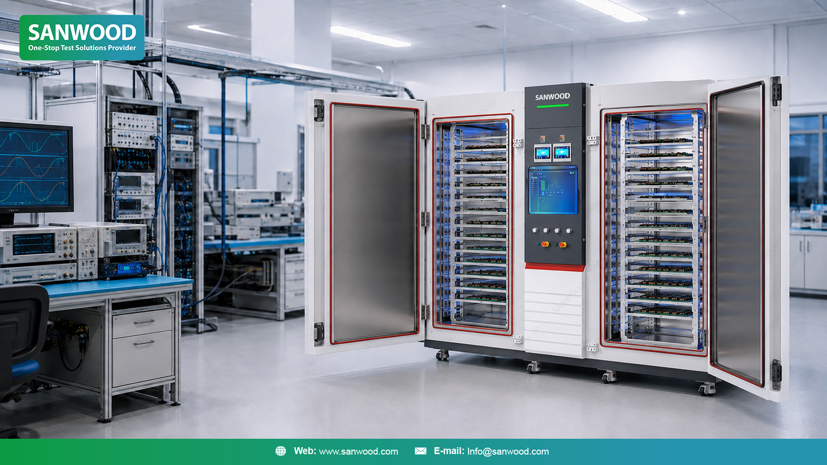
Static high-temperature storage can show whether a device survives thermal exposure. It does not show whether the device behaves correctly while it is operating under that stress.
Memory and MCU devices are active components. They read, write, switch, compare, address, output, receive and respond to digital patterns. A device may pass a short room-temperature test, then show unstable behavior during high temperature operation.
A Memory Burn-in Test System helps find issues such as:
• Memory read/write instability during high temperature aging
• MCU pin or logic response drift under powered stress
• SoC digital chip behavior changes during dynamic aging
• FLASH or DRAM abnormal response under long-duration aging
• Lot-level variation that does not appear in a short functional check
• Marginal devices that need early separation before shipment or integration
The purpose is not only to heat the device. The purpose is to observe whether the device remains logically stable while heat and electrical operation are applied together.
SANWOOD's chamber-temperature-controlled integrated circuit high temperature dynamic aging system is intended for low and medium power semiconductor devices, especially devices with power consumption up to 10 W.
Typical device categories include:
• Memory ICs
• FLASH memory devices
• DRAM devices
• Small and medium-scale MCU devices
• Digital logic devices
• SoC digital chips
• Storage-related ICs
• Low-power semiconductor devices requiring dynamic aging
Typical package forms may include:
• QFN
• QFP
• BGA
• SOP
• SSOP
• TSSOP
This device scope matters because the system should be matched to the semiconductor device type, package form, power level and dynamic test requirement instead of being treated as a generic chamber.
The system supports high temperature dynamic aging in a controlled environment from room temperature +10℃ to +150℃, depending on the project configuration, device requirement, board design and test method.
This is the environmental side of the system. It is why the product belongs in the wider SANWOOD portfolio of environmental test chamber and climatic test chamber solutions.
However, temperature range should not be the only selection factor. For memory and MCU dynamic aging, the chamber must work together with the electrical test architecture. Temperature control, board layout, heat load, cable routing, airflow consistency and data communication all affect the usefulness of the final aging result.
TDBI is the key difference between simple thermal exposure and dynamic aging.
With TDBI, the device under test can be logically exercised during high temperature aging. The system can output patterns, drive signals, compare responses and help engineers identify failures that appear only while the device is active.
For semiconductor reliability teams, this creates a more useful test window:
• Before aging: initial electrical and functional state
• During aging: dynamic logic behavior under thermal stress
• After aging: recovery, drift, failure confirmation or lot comparison
The "during aging" layer is the reason a Memory Burn-in Test System is more valuable than a chamber-only setup for many Memory IC and MCU projects.
For dynamic aging, electrical capability is as important as thermal control. SANWOOD's system can be configured around the following signal and test performance points:
• Single-board signal channels: 184 I/O
• Maximum programming depth: 64M Words Max
• Maximum signal frequency: 20 MHz
• Edge types: 8 Edges
• Vector edge formats: 8 basic formats, including D/U/Z/P and L/H/X/T
• Digital signal drive level: VIH = 0.6 V to 5.5 V, VIL <= 0.8 V
• Drive current capability: +/-200 mA
• Output signal edge attribute: Tr <= 10 ns, Tf <= 10 ns
• Window comparator reference level range: VOH 0.6 V to 5.5 V, VOL 0.6 V to 5.5 V
For vector edge format references, D can indicate output low level, U output high level, Z output high impedance and P output hold. L can indicate received low level, H received high level, X receiving don't-care state and T received high impedance.
These details should be confirmed against the actual device, board and test program. They are included because they help engineers evaluate whether the system is suitable for a specific Memory IC, MCU, SoC, FLASH or DRAM aging task.
A standard environmental test chamber creates a controlled environment. A Memory Burn-in Test System creates a controlled environment and checks device behavior while the device is active.
The difference is important:
• A chamber-only test can expose the device to temperature.
• A dynamic aging system can expose the device to temperature and electrical operation.
• A TDBI-enabled system can expose the device to temperature, electrical operation and logic function verification.
For semiconductor projects where the failure mechanism depends on powered behavior, the third option is the most useful.
This does not make standard climatic test chambers less important. It simply means they answer a different question. A climatic chamber is useful for environmental exposure. A memory burn-in system is useful for active semiconductor aging and screening.
The system may be considered for:
• Memory IC burn-in and aging
• FLASH reliability screening
• DRAM high temperature aging
• MCU powered dynamic aging
• SoC digital chip logic aging
• Digital logic device validation
• Low-power IC life evaluation
• Process comparison across semiconductor lots
• Engineering validation before production screening
• Failure analysis support after abnormal electrical behavior
For automotive electronics, industrial control, storage-related modules and embedded systems, this type of test can help teams understand device behavior before the IC becomes part of a higher-value assembly.
Memory burn-in and high temperature dynamic aging projects are usually planned according to the device type, application field and customer qualification method. The Memory Burn-in Test System provides the controlled temperature environment and electrical test capability, while the actual test profile should be confirmed against the applicable standard, customer specification or internal reliability plan.
Commonly referenced international standards and methods may include:
• JEDEC JESD47 for stress-test-driven qualification of integrated circuits
• JEDEC JESD22-A108 for temperature, bias and operating life test methods often associated with high temperature operating life evaluation
• JEDEC JESD22-A103 for high temperature storage life when passive storage stress is part of the reliability plan
• AEC-Q100 for failure-mechanism-based stress test qualification of packaged integrated circuits used in automotive applications
• AEC-Q100-008 for early life failure rate evaluation when infant-mortality screening is required
• AEC-Q100-005 for non-volatile memory program/erase endurance, data retention and operational life considerations
• IEC 60068-2-2 for dry heat environmental testing of components, equipment or other articles
• IEC 60068-2-14 for change of temperature when the test plan includes temperature transition stress
• ISO 16750-4 for climatic load references in road vehicle electrical and electronic equipment projects
These references are not interchangeable. JEDEC and AEC documents are often used for semiconductor qualification and device-level reliability planning, while IEC and ISO methods are more common in broader environmental and application-level validation. A memory burn-in system should therefore be configured around the required temperature condition, TDBI logic test method, device package, electrical stress and pass/fail criteria defined by the applicable test plan.
Before specifying a Memory Burn-in Test System, prepare the device and test information first:
• Device category: Memory IC, FLASH, DRAM, MCU, SoC, logic IC or other low-power IC
• Package type: QFN, QFP, BGA, SOP, SSOP, TSSOP or other package
• Device power level and heat load
• Required temperature profile and aging duration
• I/O count and pin coverage
• Pattern depth and signal frequency
• Required drive voltage and drive current
• Comparator reference level requirements
• TDBI logic function test requirement
• Applicable standards, customer specifications or internal reliability methods
• Board, socket and fixture design
• Pass/fail recording and abnormal channel tracking
• Communication, data export or factory integration needs
This information helps determine whether the standard system configuration is enough or whether the electrical, thermal or mechanical design should be customized.
SANWOOD Technology provides environmental test chamber, climatic test chamber and semiconductor reliability test system solutions for memory, MCU, storage, automotive electronics, industrial electronics and advanced electronics customers.
For Memory Burn-in Test System projects, SANWOOD can help review:
• Device type and package form
• Low-power IC aging requirement
• TDBI test requirement
• Signal channel and pattern depth needs
• Drive-level and comparator settings
• Chamber temperature control and airflow design
• Board, socket and fixture layout
• Cable routing and system communication
• Data recording and alarm requirements
• Engineering validation or batch screening workflow
The goal is to match the thermal environment and electrical test capability to the device behavior question. For Memory IC and MCU customers, that means starting from the chip, package, pin requirement and aging purpose before finalizing the system configuration.
A Memory Burn-in Test System is a high temperature dynamic aging system for Memory ICs, MCUs, SoC digital chips, FLASH, DRAM and other low-power semiconductor devices. It combines controlled chamber temperature with electrical drive and logic function testing during aging.
High temperature storage exposes a device to heat, usually without active operation. Memory burn-in uses heat together with powered operation, signal drive, pattern output and response checking. This can reveal failures that static exposure may miss.
TDBI allows testing during burn-in. It helps engineers check whether the device remains logically stable while it is being aged at high temperature, instead of only testing the device before and after aging.
It can support low and medium power devices such as Memory ICs, FLASH, DRAM, MCUs, digital logic devices, SoC digital chips and storage-related ICs. Typical package forms include QFN, QFP, BGA, SOP, SSOP and TSSOP.
Project configurations may support a controlled environment from room temperature +10 C to 150 C. The final temperature condition should be confirmed based on the device, board, heat load and test method.
It is both. The chamber side provides the controlled temperature environment, while the TDBI and signal system provide electrical drive, vector output and response comparison. That combination is what makes it suitable for dynamic semiconductor aging.
It is easier to search and closer to buyer language. "High Temperature Dynamic Aging Test System" should still be used as the technical descriptor because it explains the engineering method and supports technical search queries.
A suitable Memory Burn-in Test System should be selected from the device requirement, not only from the chamber temperature range. For Memory ICs, MCUs, SoC digital chips, FLASH and DRAM devices, the key details include package form, I/O count, pattern depth, signal frequency, drive level, comparator requirement, temperature profile and TDBI test method.
SANWOOD can help review both sides of the project: the environmental test chamber conditions needed for high temperature dynamic aging, and the electrical test capability needed to drive and verify the device during aging.
For teams planning memory burn-in, MCU dynamic aging, FLASH or DRAM reliability screening, sharing the device type, package, test pattern, operating temperature, board design and data recording needs will make the system configuration more accurate from the start.
Sanwood is not just a company; it is a commitment to delivering high-quality products that stand the test of time.

 English
 中 文
中 文


 info@sanwood.com